Makonis Semicon
  • Home
  • About Us
  • Contact
  • RTL Design
  • Design Verification
  • Analog Design
  • Analog Layout
  • Physical Design
  • Static Timing Analysis
  • Physical Verification
  • DFT
  • Home
  • About Us
    • RTL Design
    • Design Verification
    • Analog Design
    • Analog Layout
    • Physical Design
    • Static Timing Analysis
    • Physical Verification
    • DFT
  • Contact
Engineer reviewing a VLSI chip design on a laptop

Physical Design

Our Physical Design services transform verified RTL into optimized, manufacturable silicon through a complete implementation flow. By focusing on performance, power, area (PPA), and timing optimization, we deliver high-quality layouts that meet stringent design and manufacturing requirements. Our expertise ensures efficient implementation and accelerates the path to successful tape-out.

About Our
Physical Design Service

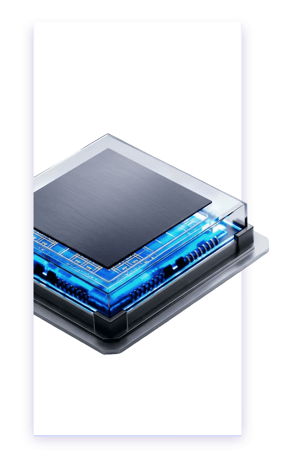
Rendered semiconductor chip package
  • End-to-End Implementation

    We manage the complete physical design flow, from floorplanning and placement to routing, optimization, and final sign-off.

  • PPA Optimization

    Our engineers optimize power, performance, and area (PPA) to deliver efficient, high-performance silicon solutions.

  • Timing & Quality Assurance

    Through timing closure, congestion analysis, and signal integrity optimization, we ensure robust and reliable chip implementation.

  • Tape-Out Ready Designs

    Our comprehensive physical design process delivers manufacturable, sign-off-ready silicon that accelerates product development and improves first-pass success.

Key Features

Floorplanning & Power Planning

Optimized floorplans and power distribution for efficient chip implementation.

Placement & Clock Tree Synthesis (CTS)

Accurate cell placement and clock network optimization for superior timing performance.

Routing & Optimization

High-quality routing with timing, congestion, and signal integrity optimization.

Physical Sign-Off

Complete implementation with timing closure and tape-out-ready design verification.

Looking for
VLSI Design Services?

Whether you’re building the next breakthrough chip or scaling an existing design, our experts are ready to help.


Services that accelerate
silicon success.

Our semiconductor engineering services combine innovation, technical expertise, and quality to deliver reliable silicon solutions that reduce development time and accelerate your path to market.

  • Home
  • About Us
  • Services
  • Contact

Corporate Office
51, 3rd Cross Rd, Aswath Nagar
Marathahalli, Bengaluru
Karnataka 560037
Get In Touch

info@makonissemicon.com
+91 8041707838

Socials
  • Linkedin
  • Facebook
  • Instagram
  • X

Copyright © Makonis Semicon Pvt. Ltd. 2026