Makonis Semicon
  • Home
  • About Us
  • Contact
  • RTL Design
  • Design Verification
  • Analog Design
  • Analog Layout
  • Physical Design
  • Static Timing Analysis
  • Physical Verification
  • DFT
  • Home
  • About Us
    • RTL Design
    • Design Verification
    • Analog Design
    • Analog Layout
    • Physical Design
    • Static Timing Analysis
    • Physical Verification
    • DFT
  • Contact
Engineer reviewing a VLSI chip design on a laptop

DFT

Our Design for Testability (DFT) services ensure that integrated circuits are optimized for efficient testing and high manufacturing yield. By incorporating advanced test architectures early in the design cycle, we improve fault detection, simplify diagnostics, and enhance product reliability. Our DFT expertise helps deliver production-ready silicon with confidence and first-pass success.

About Our
DFT Service

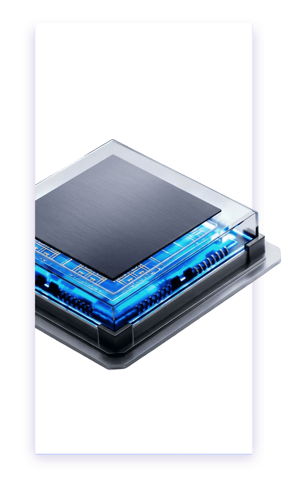
Rendered semiconductor chip package
  • Robust Test Architecture

    We design scalable DFT solutions that enhance chip testability while minimizing impact on performance, power, and area.

  • High Fault Coverage

    Our ATPG and scan methodologies ensure comprehensive fault detection, improving product quality and manufacturing reliability.

  • Efficient Manufacturing

    By implementing industry-standard DFT techniques, we reduce testing complexity, optimize production, and increase silicon yield.

  • Production-Ready Silicon

    Our end-to-end DFT services help customers achieve faster test development, reduced manufacturing costs, and successful first-pass silicon.

Key Features

Scan Insertion

Implementation of full-scan and partial-scan architectures for improved fault coverage.

ATPG & Fault Coverage

High-quality Automatic Test Pattern Generation (ATPG) to maximize defect detection.

Built-In Self-Test (BIST)

Integration of Memory BIST (MBIST) and Logic BIST (LBIST) for efficient on-chip testing.

Testability Optimization

DFT methodologies that improve manufacturing yield, diagnostics, and production efficiency.

Looking for
VLSI Design Services?

Whether you’re building the next breakthrough chip or scaling an existing design, our experts are ready to help.


Services that accelerate
silicon success.

Our semiconductor engineering services combine innovation, technical expertise, and quality to deliver reliable silicon solutions that reduce development time and accelerate your path to market.

  • Home
  • About Us
  • Services
  • Contact

Corporate Office
51, 3rd Cross Rd, Aswath Nagar
Marathahalli, Bengaluru
Karnataka 560037
Get In Touch

info@makonissemicon.com
+91 8041707838

Socials
  • Linkedin
  • Facebook
  • Instagram
  • X

Copyright © Makonis Semicon Pvt. Ltd. 2026